Analog Circuit – refers to an electrical circuit providing a continuous quantitative output as a response from its input.
Automated Test Equipment (ATE) – automated equipment designed to analyze and test the functional parameters and evaluating performance of a tested electronic device.
Built-In Self Test - an electrical testing method allowing tested devices to test themselves with specific hardware.
CAD - Abbreviation for Computer Aided Design. CADs are computer programs to design circuitry patterns and circuit boards electronically rather than physical drawing or drafting.
CAM - Abbreviation for Computer Aided Manufacturing Software of programs designed to simulate and check the manufacturability of a product.
Chip - an individual circuit or component of a silicon wafer, the lead-less form of an electronic component.
Design For Manufacturing (DFM) – a process to check that the design fits the fabrication process requirements and checks for minimal trace width, minimal trace-to-trace distance, minimal hole clearance, as well as additional information.
Dielectric - the insulating material between conductors.
DIP - dual in-line package with two rows of leads from the base in standard spacing between the leads and row. DIP is a through-hole mounting package.
DRC - Design Rule Check.
Dry Film Resist - an ultraviolet light sensitive photopolymer (photoresist) used in the imaging process
Edge Connector – is a connector on the circuit substrate edge in the form of plated pads or lines of coated holes used to connect other circuit board or electronic device.
Electronic Component – is a part of the printed circuit board, including resistors, capacitors, transistors, etc.
ENIG - Abbreviation for Electro-less Nickel Immersion Gold
Fine Pitch – also called surface-mount components with a lead pitch of 25 mils or less.
Footprint – refers to the size and shape of the pads for soldering certain electronic component.
Functional Test - the electrical testing of an assembled electronic device with simulated function generated by the test hardware and software.
Gerber File – a commonly used file used in controlling a photo-plotter.
Ground Plane - a conductive plane as a common ground reference in a multi-layer board for current returns of the circuit elements and shielding.
IC – the abbreviation for an Integrated Circuit.
In-Circuit Test – is the electrical testing of individual components or parts of a circuit board rather than testing the whole circuit.
Lamination - Many printed circuit boards are made up of multiple layers, these are referred to as multi-layer printed circuit boards. They consist of several thin etched boards or trace layers and are bonded together through the process of lamination.
Lead-free finishes -refer to a variety of lead-free finishes available today that meet RoHS compliance but it is important to understand the pros and cons of each finishing option and which to choose for your application.
Leakage Current - A small amount of current that flows across a dielectric area between two adjacent conductors.
Legend – Letters, numbers or symbols that are printed on a circuit board which may include part numbers and product number or logos.
Minimum Conductor Width – refers to the minimum width of any conductors, such as traces, on a board.
Minimum Conductor Space - The minimum distance between two adjacent conductors, such as traces, on a circuit board.
Net – refers to a set of pads to be connected electrically on the board.
Netlist - List of parts and their connection points which are connected in each net of a circuit.
NPTH – Abbreviation for Non-plated through-hole.
Pad – refers to the metalized or plated area of the board for connection and attachment of electronic components.
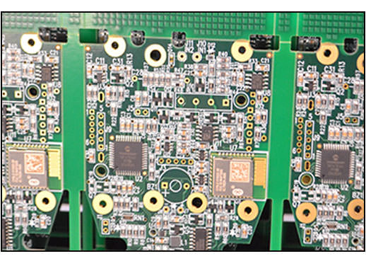
PCB - Abbreviation for Printed Circuit Board.
PWB – Abbreviation for Printed Wiring Board ( an older term for PCB)
Pin – or pinout is a part of an electronic component which is soldered to the board.
Pitch – refers to the center-to-center spacing between conductors, such as pads and pins, on a board.
PTH -Abbreviation for (plated-through hole) which is a plated hole used as a conducting interconnection between different layers or sides of a board either used as connection for through-hole component or as a via.
RoHS - Abbreviation for Restriction on Use of Hazardous Substances, RoHS restrictions took effect on July 1, 2006.
Routing (tracing) - the process of placing electronic connections (traces) between pads on the board.
Signal layer - layer of a board, in which traces can be placed. For a two-sided board two signal layers are available - the Top and the Bottom layers.
Silk screen - a layer designed for placing legend elements on the top or bottom side of the board. Two corresponding layers are available - the Top Silk and the Bottom Silk.
Small Outline Integrated Circuit (SOIC) - an integrated circuit with two parallel rows of pins in surface mount package.
SMD - Abbreviation for Surface Mount Device .
SMT - Abbreviation for Surface Mount Technology .
Substrate - circuit board layers are separated by a substrate which is a laminated insulator that separates the circuitry design
Test Point – is a specific point on a circuit board used to test functional adjustment or quality test in the circuit-based device.
Thermal pad – is a special form pad used when it is connected to copper pours. Thermal pads improve the soldering of a joint and reducing the chance of a cold solder joint.
Through-hole – refers to a drilled hole in the board, usually for mounting purposes.
Trace (or Route) - a layout or wiring of an electrical connection.
UL - Underwriters Laboratories. A popular safety standard for electrical devices supported by many underwriters.
Via or VIAS – refers to a plated-through hole used for interconnection of conductors on different sides or layers of a circuit board.
Wave Soldering – is when solder joints are soldered simultaneously using a wave of molten solder.

